The Industrial Science Report: 3D printing drives programmable industrial materials and new levels of process control
Key Highlights
- Materials like copper are now engineered through additive manufacturing to disintegrate or remain stable on demand.
- Direct 3D printing of nanolasers onto semiconductor chips offers a flexible alternative to traditional lithography.
- Innovative techniques engineer defects within energetic materials to precisely tune ignition and combustion properties.
- Hybrid super foam uses in-foam additive manufacturing to create lightweight, energy-absorbing structures suitable for protective gear, automotive safety, and noise reduction.
- Biomimetic nozzles inspired by mosquito proboscises enable ultra-fine, cost-effective 3D printing for tissue engineering and regenerative medicine.
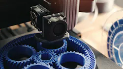
A few weeks ago in The Industrial Science Report, I wrote about material development research in the automotive industry, which was largely moving away from trial-and-error experimentation, toward data-driven and predictive design, as well as processes that command more control over material development to key in on certain performance characteristics as it forms. This week’s collection of additive manufacturing research adds to the theme of programmable materials, where metals like copper are engineered to remain stable or self-destruct on command, nanolasers for data processing are printed directly onto microchips, and energetic materials are designed to control ignition parameters and safety.
We see a similar concept with hybrid foams that dynamically redistribute impact forces and even bio-inspired 3D printing nozzles that slash costs while improving precision. Additive manufacturing is a key technology for engineering materials at the microstructure level. For manufacturers, these new materials could experience fewer equipment failures, but also add a new responsibility to understand, monitor, and maintain materials that have dynamic properties.
Porous copper 3D printing unlocks material behavior for security and energy
Copper is ubiquitous in industry and a long-time staple of electronics and energy systems for its electrical conductivity, strength, and durability. Recently, researchers have developed a copper material via additive manufacturing that would fall apart in oxygen. But what seemed like a failed experiment turned into an opportunity.
Arizona State University’s work with the high-resolution continuous 3D-printing process, micro continuous liquid interface production or µCLIP, can create copper parts that are either rock-solid or engineered to fall apart on command, depending on how they control printing and sintering (a high temperature thermal process that bonds compacted metal without reaching their melting point).
When scientists discovered a copper that disintegrated when exposed to air, they realized they could engineer a material to intentionally oxidize and fail for new applications in information security and secure devices, such as a computer or cell phone chip that would be tamper-proof or protected from sensitive information access.
For maintenance and reliability engineers, this is more than a cool spy trick. It’s a look at the next level of functional materials, where you might design components that signal tampering or degrade safely under certain conditions. Additive processes are giving manufacturers unprecedented control over how a metal behaves at the nanoscale.
Arizona State University (ASU) researchers developed a method to 3D print complex, nanoporous copper structures using a high-resolution additive manufacturing process that influences the material’s microstructure and properties. By carefully controlling printing and heating steps, they can tune copper between dense stable forms and reactive nanoporous states, giving manufacturers new control over performance and functionality. This includes potential built-in protective behaviors, where exposure to air triggers structural changes that could serve information security purposes, and energy-related uses through increased surface area and reactivity. The study, supported by the National Science Foundation (NSF) Future Manufacturing funding, signals a shift from shape-only additive manufacturing to functional material design across scales.
3D nanolasers support next-gen optical chips and quantum security
If copper showed us materials can be programmed, this work shows how additive manufacturing is building that control directly into semiconductor fabrication too. Researchers are now printing lasers directly onto semiconductor chips, as a viable path around the physical and economic limits of lithography. With additive approaches and by moving from horizontal to vertically printed nanolasers, this sidesteps lithography’s rigidity and opens the door for higher-density optical components.
Test your industry knowledge.
Quiz: How AI is reshaping industrial productivity, sustainability, and resilience?
Need to study? Read the article.
Nanolasers are gaining attention for the next-generation of semiconductors that are needed to support the high-speed optical computers for massive artificial intelligence scale-up, quantum cryptographic communication (using quantum mechanics for secure data transmission), and ultra-high-resolution augmented reality displays. The nanolasers can process information using light in spaces thinner than a human hair. With the appetite for compute density only growing, high efficiency, high density methods will go a long way.
The process uses perovskite, a class of crystalline materials with a distinctive atomic structure that enables highly efficient light emission and absorption, making it especially promising for advanced semiconductor, security, and energy applications.
Conventional lithography is limited by its planar, subtractive nature, making it complex and costly. A light-based patterning process transfers complex circuit designs onto silicon wafers, and the process is poorly suited for fabricating vertical nanostructures with the flexibility needed for spatial control over light-emitting components.
At industrial scale, nanolaser production will require a new set of process domains and failure points for maintenance and reliability teams in semiconductor manufacturing. Pervoskite crystal quality, light conditions, and precision alignment at the nanoscale will drive on-chip optical components.
A joint research team from the Korea Advanced Institute of Science and Technology (KAIST) and Pohang University of Science and Technology (POSTECH) has developed an ultra-fine 3D printing process that directly fabricates vertical nanolasers onto semiconductor chips, aiming to overcome spatial and efficiency limits of conventional lithography. The method uses ultra-fine electrohydrodynamic 3D printing to stack perovskite structures with near single-crystalline alignment, increasing nanolaser efficiency with controlled light emission and minimal loss. The vertically printed structures achieve tuned laser colors via height adjustment, enabling applications in optical computing, quantum cryptographic communication, and potential anti-counterfeiting technology. The original research was published in ACS Nano.
New 3D printing techniques improve safety and control of energetic materials
This work pushes the idea of programmable materials further by engineering defects themselves as a controlled variable. We don’t usually think of imperfections as something you’d intentionally design into a process, but in the case of energetic materials (explosives, pyrotechnics, and propellants), this new 3D printing technique might make products that are safer than the original. Traditionally, energetic materials are manufactured through casting or milling processes. This is ideal for large batch production, efficient and scalable. However, these processes struggle with customization, which limits innovation and performance in designing better materials.
This work from Purdue University is using additive manufacturing to engineer pores into energetic materials, which allow manufacturers to directly tune how and when ignition happens, rather than relying on variability. The placement of defects or pores in the material either increases or decreases the likelihood of ignition when subjected to friction, impact, extreme temperature, or other conditions.
Additive manufacturing gives researchers the freedom to experiment and customize, and tune the materials specific properties, such as burn rate and blast shape.
At Purdue University, mechanical engineering researchers led by Monique McClain are advancing additive manufacturing techniques to control the behavior of energetic materials at the particle and structural levels. Their work focuses on how manufacturing (binder choice, mixing, microstructure design) influences performance, sensitivity, and safety, enabling deliberate pore engineering to tune ignition and combustion properties. Additive methods allow more complex geometries and material combinations than traditional casting or milling, unlocking new pathways for safer customization. The research team also developed a patent-pending process for polymer-bonded explosive powders that reduces waste and improves uniformity. The research is sponsored by the U.S. Air Force Office of Scientific Research’s Young Investigator Research Program and the Army Research Office Energetic Materials Basic Research Center.
Hybrid super foam enables tunable energy-absorbing materials for advanced manufacturing
What we’ve seen in metals, semiconductors, and energetic materials now shows up in a very familiar product. Foam, too, can be tuned and programmed for performance. According to researchers at Texas A&M, using energy-absorbing materials typically meant either choosing cheap foam that’s inconsistent, or engineered lattice foams that are very expensive. Ordinary foams have random and chaotic internal structures that limit how efficiently they absorb energy, and engineered foams perform better at a much higher price point.
Researchers now think the solution to this trade-off is in-foam additive manufacturing (IFAM), which effectively programs performance into a low-cost material. It uses a 3D strut network to stabilize and then redistribute loads as conditions change.
During early compression, the foam braces the struts and keeps them steady so they don’t buckle. As the pressure builds, the struts take over and spread the load outward to the surrounding foam. This material teamwork allows the composite to absorb more energy and greater forces.
The U.S. Army is interested in energy-absorbing materials for ballistic helmets and blast-resistant seat cushions, and the foam also has consumer applications, such as lining car bumpers and interiors. Researchers say it also has potential for noise control.
A better, cheaper foam could benefit all manufacturers from a maintenance perspective. Stronger, more efficient foam means fewer premature failures on fleet equipment and PPE, especially in applications like seating, protective equipment, or machine guarding where repeated compression cycles matter. It’s a reminder that smarter materials design upstream can eliminate many downstream maintenance headaches.
Researchers at Texas A&M University, in collaboration with the DEVCOM Army Research Laboratory, have developed a hybrid “super foam” using a manufacturing approach called in-foam additive manufacturing (IFAM). The process embeds a 3D-printed elastomeric skeleton of plastic struts into conventional foam, enabling a composite that can absorb up to 10 times more energy than standard padding while remaining lightweight and low-cost. By controlling parameters such as strut geometry, spacing, and elasticity, the material can be tuned for specific performance characteristics including strength, energy absorption, and comfort. The research shows how combining additive manufacturing with traditional materials can overcome tradeoffs between cost and performance, making advanced energy-absorbing structures more viable for large-scale production. Target industries include defense (helmets, blast-resistant seating), automotive (vehicle safety systems), aerospace (impact and acoustic applications), and consumer products such as protective gear and cushions.
Researchers use mosquito proboscis as ultra-fine 3D printing nozzle
Additive manufacturing is redefining materials from the inside out, and this research highlights important innovations to the additive process, reshaping the smallest, most failure-prone tools in the whole process. Perhaps the best solution to precision, cost, and durability isn’t always better engineering. Ask researchers at Drexel University and McGill University, who are borrowing from nature instead.
One of nature’s most annoying features, the proboscis, which a mosquito uses to suck our blood, might make a better needle-like structure as the tip of a 3D printer, than manufactured dispense tips, especially for printing microscopic structures, finer than a human hair. This type of precision is needed for manufacturing tissue samples used in regenerative medicine, drug screening, and cancer treatment.
According to the research, current 3D printed dispense tips used to produce tissue samples cost as much as $80 a piece to the tune of billions of dollars a year in the U.S. alone. The mosquito proboscis can be repurposed for about 80 cents. For manufacturing, “necroprinting,” or using a non-living biological structure as an advanced manufacturing tool, suggests a radically different supply chain. For maintenance and reliability professionals, 3D bioprinting using a proboscis as a biodegradable, submicron dispense tip could redefine replacement strategy and inventory management.
Researchers at Drexel University and McGill University repurposed the feeding tube (proboscis) of mosquitoes as a biological dispense tip for high-definition 3D printing, achieving line widths finer than a human hair. The process uses natural microstructures as biodegradable, affordable nozzles that outperform conventional glass tips in printing accuracy, longevity, and cost. Demonstrations included microscopic structures and tissue scaffolds, including red blood cell-laden bioinks, showing potential to improve bioprinting and materials fabrication for regenerative medicine and drug testing. The work highlights a biomimetic (or emulating natural models, systems, and processes) route to precision manufacturing by repurposing evolved biological tools for engineering applications.
About the Author

Anna Townshend
managing editor
Anna Townshend has been a journalist and editor for almost 20 years. She joined Control Design and Plant Services as managing editor in June 2020. Previously, for more than 10 years, she was the editor of Marina Dock Age and International Dredging Review. In addition to writing and editing thousands of articles in her career, she has been an active speaker on industry panels and presentations, as well as host for the Tool Belt and Control Intelligence podcasts. Email her at [email protected].