The Industrial Science Report: Data-driven materials development focuses on manufacturing speed, precision, and reliability
Key Highlights
- Scientists are leveraging AI, quantum modeling, and large-scale simulations to accelerate the discovery and optimization of new materials with targeted properties.
- Atomic-scale control during additive manufacturing allows for in situ tuning of microstructures and stronger, more ductile metals.
- AI models like large language models are drastically reducing design cycles for optical metasurfaces.
- Tunable metamaterials are being engineered to actively respond to environmental stimuli, enhancing sensing, energy management, and communication systems.
- Innovative fabrication methods use femtosecond laser writing to create programmable nanostructures inspired by biological surfaces, with applications in ultra-sensitive sensing.
One theme keeps resurfacing as I work through The Industrial Science Report lately: scientists and engineers are pushing materials into new territories, and new materials are increasingly designed, tuned, and programmed, even at nanoscale. Across research from Northwestern University McCormick School of Engineering, Lawrence Livermore National Laboratory, Penn State University, Swinburne University of Technology, and the Chinese Academy of Sciences, predictive, AI-driven design is collapsing development timelines; additive processes are enabling atomic-level control during production; and entirely new classes of materials—from metasurfaces to metamaterials to self-organizing nanostructures—are blurring the line between material and system.
What stands out to me isn’t just the amazing science, but the trajectory for industry: shorter R&D cycles, more data-intensive production, and assets that increasingly embed sensing and control into their very structure.
Northwestern predictive and data-driven material design accelerates manufacturing innovation
In looking specifically at new material design for the automotive industry last week, it was clear that the discovery process has moved from trial-and-error to predictive and data-driven. At Northwestern University McCormick School of Engineering, that same shift is taking shape through integrated quantum-mechanical modeling, AI, and large-scale computational frameworks that screen both known and hypothetical materials for stability, performance, and sustainability characteristics. It’s a pipeline for engineering materials with targeted electronic, optical, and mechanical properties, supporting the development of longer-lasting batteries, more efficient electronics, lighter aerospace components, and stronger, more sustainable structures.
For industrial development, this replaces one of the most persistent cost centers: the trial-and-error process. In its place is predictive insight that can shorten design cycles, improve reliability, and reduce material-related failures in the field. For maintenance and reliability teams, more data-intensive production environments will demand equally advanced monitoring, calibration, and control strategies to ensure equipment can consistently deliver these engineered outcomes.
At the Northwestern University McCormick School of Engineering, researchers are integrating quantum-mechanical modeling, AI, and predictive data-driven methods to transform material design and manufacturing. University professors use atomic-scale simulations to screen and design materials with targeted properties, significantly reducing development time and eliminating costly trial-and-error experimentation. Computational frameworks developed at McCormick rapidly optimize material compositions and predict performance, enabling the creation of stronger, lighter, and more sustainable materials for aerospace, batteries, and other applications. Initiatives such as the National Science Foundation (NSF)-sponsored HAMMER ERC and NIMSI collaborative hub aim to connect materials discovery directly with advanced manufacturing processes, supporting real-time control and rapid customization of material properties. This integrated approach is positioned to accelerate technology transfer from lab discovery to industrial deployment.
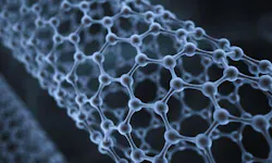
Atomic-scale control opens the door to tailored metals for advanced manufacturing
If predictive modeling is rewriting how materials are designed, the next question is whether those insights can survive the factory floor. At Lawrence Livermore National Laboratory, researchers are showing that they can with additive manufacturing. They are controlling material behavior not just in simulation, but in the moment of fabrication itself. By adjusting laser scan speed in high-entropy alloys, the team can dictate how atoms settle during solidification, effectively locking in desired properties like strength or ductility at the atomic scale. For manufacturers, that turns additive manufacturing from a process constrained by legacy materials into one where performance is engineered in situ. For maintenance and reliability teams, it signals a shift toward equipment that must consistently deliver precise thermal and deposition conditions to achieve those engineered outcomes.
Scientists at Lawrence Livermore National Laboratory and collaborators have demonstrated a method to engineer next-generation materials for additive manufacturing by controlling atomic structures during the 3D printing of compositionally complex alloys. By tuning the laser scan speed during printing, the team showed that cooling rates can be manipulated to “freeze in” desirable microstructures that yield a spectrum of mechanical properties, from high strength to greater ductility. The research combined thermodynamic modeling and molecular dynamics simulations to predict how atoms settle during solidification, overcoming longstanding challenges in predicting mechanical behavior of metals from additive manufacturing. This atomic-scale control could transform additive manufacturing from a process limited by legacy alloys into a platform for designing materials with tailored properties for aerospace, national security, and commercial industries.
Penn State researchers use large language models to accelerate metasurface design for optical systems in healthcare, defense, and consumer electronics
A design cycle that once took months can now unfold in milliseconds, again transforming the trial-and-error scientific process with AI-driven analytics. At Penn State University, researchers are applying large language models (LLMs)—a subset of deep learning architectures built on neural networks—to predict light–matter interactions in metasurfaces with unprecedented speed. Traditional neural networks require extensive tuning and trial-and-error to arrive at accurate models, and deep learning scales that approach through layered architectures. However, LLMs go a step further by leveraging pre-trained, highly generalized pattern recognition to bypass much of that configuration overhead entirely. For manufacturers of optical and nanophotonic systems, this translates into dramatically shorter R&D cycles, faster prototyping, and a more direct path from design to deployable components in applications ranging from imaging and sensing to advanced display technologies.
Penn State researchers have developed a rapid, AI-driven method for designing engineered materials that manipulate light at the nanoscale. By using large language models (LLMs), the team can predict how light interacts with metasurfaces in seconds, replacing months-long traditional simulations and neural network setups. Trained on a data set of more than 45,000 metasurface designs, LLMs were very accurate predicting in a short time how a metasurface will interact with light. This approach enables highly customized metasurface designs for applications in camera lenses, virtual reality headsets, holographic imagers, and other advanced optical systems. The research, featured in Nanophotonics, supports the integration of nanophotonic devices into industries such as healthcare, defense, energy, and consumer electronics.
Swinburne University researcher award advances tunable wave metamaterials for manufacturing and sensing
Speeding up design is only part of the shift. Increasingly, materials are being engineered to actively shape how energy and signals move through a system, more infrastructure than material. That’s the focus of new work at Swinburne University of Technology, where tunable metamaterials are designed to “listen” and respond to their environment. Unlike conventional materials, metamaterials derive their properties from precisely engineered structures rather than chemistry, and this project applies topology-optimization frameworks to automatically discover architectures that concentrate and direct energy with specific frequency responses.
For industry, that opens a path toward materials that function as part of the sensing, communication, and energy infrastructure itself and possibly overcoming the limitations of traditional waveguides, sensors, and energy harvesters. In practical terms, manufacturers could see components that inherently filter noise, sharpen signal fidelity, or capture and redirect energy within systems. At scale, these capabilities point toward assets where sensing, transmission, and control are embedded directly into the material architecture.
Swinburne University physicist Dr. Weibai Li received a Discovery Early Career Researcher Award (DECRA) from the Australian Research Council and $526,081 in funding develop tools for designing tunable wave metamaterials for energy concentration. The project will create computational frameworks and algorithms that automatically discover metamaterial structures with tailored frequency responses, enabling engineered materials with advanced control over wave phenomena relevant to sensing, energy harvesting, and communications. Beyond modeling, the project includes the fabrication and characterization of next-generation metamaterials that could overcome limitations of existing waveguides and sensors in industrial applications. This research may enable manufacturable metamaterials with broadly tunable properties for advanced manufacturing and energy systems integration.
Chinese Academy of Sciences develops light-guided, programmable 3D nanowrinkles for sensors and bio-inspired materials
Wrinkles serve a purpose in nature, controlling how surfaces interact with light, liquids, and living cells. Researchers at the Chinese Academy of Sciences are experimenting with using light to build materials that organize themselves to mimic biological structures like cicada wings or intestinal microvilli. Central to this approach is the Turing process—a reaction–diffusion mechanism first described by Alan Turing—in which simple chemical interactions spontaneously generate ordered patterns. By combining femtosecond laser direct writing with Turing-style reaction–diffusion processes, the team can program 3D nanowrinkles whose orientation and spacing are dictated by laser polarization, replicating natural surface architectures, where wrinkles play a critical role in controlling interactions with light, liquids, and living cells.
For example, programmable surfaces used with silver coatings could act as ultra-sensitive Raman sensors capable of detecting trace molecules at parts-per-billion levels, enabling earlier detection of contamination or chemical changes in process environments. More broadly, the ability to translate biological surface functions into engineered materials opens new design space for anti-reflective coatings and bio-compatible, smart surfaces that interact dynamically with their surroundings.
Researchers at the Technical Institute of Physics and Chemistry, Chinese Academy of Sciences have developed a fabrication method that combines femtosecond laser direct writing with Turing self-organization to generate programmable 3D nanowrinkle patterns in soft materials. The ultrafast laser induces localized modifications that trigger reaction–diffusion dynamics, allowing controlled wrinkle formation whose orientation and periodic spacing are dictated by the polarization state of the laser. By tuning polarization, the team reproduced natural microstructures such as moth eyes, cicada wings, and intestinal microvilli, demonstrating precise control over hierarchical surface morphology.
About the Author

Anna Townshend
head of content
Anna Townshend is the chief editor and head of content for Plant Services. She has been a journalist and editor for more than 20 years and joined Plant Services and Control Design as managing editor in June 2020. Previously, for more than 10 years, she was the chief editor of Marina Dock Age and International Dredging Review. In addition to writing and editing thousands of articles in her career, she has been an active speaker on industry panels and presentations, as well as host for Great Question: A Manufacturing Podcast. Email her at [email protected].